
In the last month, I have been to the 30th anniversary of the European Conference on Radiation and its Effects on Components and Systems (RADECS) and European Symposium on Reliability of Electronic Devices, Failure Physics and Analysis (ESREF) held in Montpellier and Toulouse, respectively.
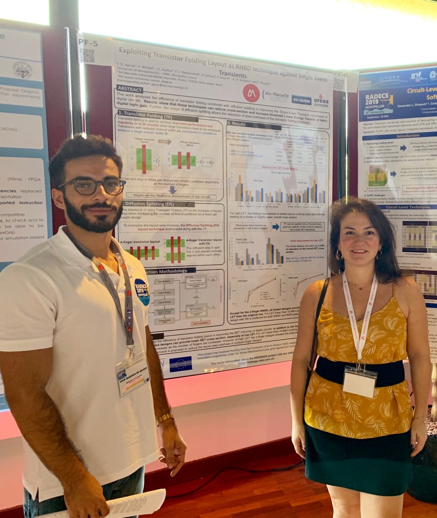
My work at RADECS is entitled “Exploiting Transisor Folding Layout as RHBD Technique against Single Event Transients” and it was presented at the poster session F (Hardening Techniques). In this work, I have analyzed the influence of folded transistor layouts on the radiation robustness of digital circuits against Single-Event Transient (SET). Besides increasing threshold Linear Energy Transfer (LET), results show that folded layouts can
also reduce the overall cross-section and the in-orbit SET rate for
protons and heavy ions in the LEO and ISS orbits.
Also at RADECS, I have contributed to another work entitled “Single Event Latchup Cross Section Calculation from TCAD Simulations – Effect of the Doping Profiles and Anode to Cathode Spacing“. In this paper, based on TCAD simulations, the Single-Event Latchup (SEL) cross-section curves were obtained according to different design modifications concerning the doping profiles and the anode-to-cathode spacing of a inverter in a commercially available bulk 65nm CMOS technology. In summary, the doping profile has shown a greater impact on the SEL sensitivity than the modifications on the anode-to-cathode spacing.
For ESREF, I have presented the paper entitled “Radiation Hardening Efficiency of Gate Sizing and Transistor Stacking based on Standard Cells“. Selective hardening techniques can be adopted in the most vulnerable nodes of complex VLSI circuits. Gate sizing is a widely used technique to achieve best delay/power trade-off in VLSI circuits. It can also be used to harden a circuit as it can increase the nodal capacitance and drive strength of the devices. Similarly, transistor stacking is able to improve hardness while providing reduction on the static power consumption. The manuscript is already published and it can be found at the Microelectronics Reliability, Elsevier: https://doi.org/10.1016/j.microrel.2019.113457

References:
Y. Q. Aguiar, F. Wrobel, J. Autran, F. Kastensmidt, P. Leroux, F. Saigné, V. Pouget, A. Touboul, “Exploiting Transisor Folding Layout as RHBD Technique against Single Event Transients,” RADECS Proceedings, IEEE, 2019.
S. Guagliardo, F. Wrobel, Y. Q. Aguiar, J. Autran, P. Leroux, F. Saigné, V. Pouget, A. Touboul, “Single Event Latchup Cross Section Calculation from TCAD Simulations – Effect of the Doping Profiles and Anode to Cathode Spacing,” RADECS Proceedings, IEEE, 2019.
Y. Q. Aguiar, F. Wrobel, S. Guagliardo, J-L. Autran, P. Leroux, F. Saigné, A. D. Touboul and V. Pouget, “Radiation Hardening Efficiency of Gate Sizing and Transistor Stacking based on Standard Cells,” Microelectronics Reliability, 2019: https://doi.org/10.1016/j.microrel.2019.113457)
